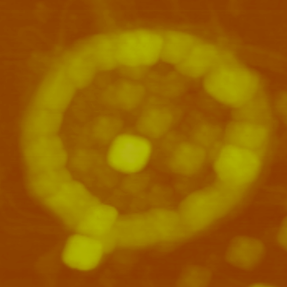
AFM /Atomic Force Microscopy
Atomic force microscopy (AFM), a type of scanning probe microscopy (SPM), is a well-established technique which offers imaging on the nanometer scale, based on the force interaction (van der Waals, electrical, magnetic, thermal etc) between a tip and a sample surface.
Multimode AFM is quite versatile and permits to gather information about any type of sample including metals, semiconductors, polymers, ceramics, composites, glass, and biological samples. Beyond the topography, many material properties can be determined including friction, electrical forces, capacitance, magnetic forces, conductivity, viscoelasticity, surface potential, and resistance.
A typical AFM consists of a cantilever with a small tip (probe) at the free end, a laser, a 4-quadrant photodiode and a scanner. It has a feedback loop using the laser deflection to control the force and tip position. A laser beam is reflected from the back of the cantilever that includes the tip. As the tip interacts with the surface, the laser position on the photodetector is used in the feedback loop to track the surface for imaging and measuring.
The facility includes 2 AFMs.


Multimode AFM with Controller Nanoscope IIIa (Digital Instruments)
Surface imaging and topographical analysis, cross-sectional profiles, roughness measurements
Contact, Tapping , Non-contact mode
2 piezoelectric scanners:
a normal for 125x125μm2 max scan size and a high precision for 5x5μm2 max scan size
1Å in z-axis, 10nm in x- and y-axis
Etched Si probes for Tapping mode, SiN probes for Contact mode
Round stubs suitable for samples up to 1cm in diameter
Lateral Force Microscopy, Magnetic Force Microscopy
Nanoscope Software v4.32r3
Katerina Tsagaraki, ktsag@physics.uoc.gr
Bruker Multimode 3D Nanoscope
Surface analysis, roughness analysis, cross-sectional profile analysis, magnetic force microscopy (MFM), size distributions, phase imaging mode.
Contact, Tapping, Magnetic Force Microscopy, non-contact mode
Scan range: from 90x90x8 μm to 125x125x10 μm (noise level 0.35Å RMS).
1Å in z-axis. Image analysis 4096 x 4096 pixels
Silicon cantilever type (TAP-300G), Silicon tip on nitride lever (SNL-10), Antimony doped silicon (RTESP), GaN probes, etc.
Two round stubs up 1 and 2 cm in diameter
Contact mode in gases and liquids, AC mode in gases and liquids, Phase Imaging mode, Lateral Force (Friction) Mode, Magnetic Force Microscopy Mode (MFM), tapping mode phase imaging, electrostatic force microscopy, kelvin probe microscopy, Force spectroscopy, PiezoResponse Microscopy
NanoScope Software 6.13
Prof. Dimitrios Gournis, dgourni@uoi.gr


