EBME / E-beam Metal Evaporation
Electron Beam (E-beam) Metal Evaporation (EBME) is a well-established physical vapor deposition technique for producing high-purity uniform metal coatings on solid or flexible substrates at a rate typically in the range of 0.1nm to 1μm/min. Basically, a high-energy electron beam (also referred to as electron gun) is used to heat the material to be deposited, which evaporates and condenses onto the substrate. EBME is a non-conformal deposition technique and thereby, it is ideal for lift-off processing compared to other techniques (magnetron sputtering, ALD, etc.). Today, ultra-thin multi-layers can be deposited via a multiple crucible system, with the ability to obtain gradient programmed compositions without breaking the vacuum. EBME is used for a wide range of applications ranging from electrical contact engineering and interconnect lines in micro/nanoelectronics to transparent conductive thin films of designed reflective and transmissive properties in optoelectronics including photovoltaics, etc.


DENTON / DV-602
e-Gun Evaporation
Metals: Al
Substrates: Semiconductors, dielectrics, resists
Resistance Evaporation Source: 2kVA, capable of 400A (at 5V) or 200A (at 10V)
Deposition rate: from 100 to 360 nm/min
From small samples of 1cm x 1cm to 4΄΄ wafers. Multi-wafer (up to six 4΄΄ or six 3΄΄ wafers) holder
Metal electrodes and interconnects of semiconductor devices, etc.
Dr. Vassilis Vamvakas, v.vamvakas@inn.demokritos.gr
TEMESCAL BJD-1800
e-Gun Evaporation
Metals: Au, Ge, Cr, Ti, Al, Ni, Pt, Ag, In, Mo, Si, Gd, Ho, Co, Zn, Sn, Cu, Mn, W, Au / Zn, Au / Ga, In / Sn, Sb, Pd, Sc, Ni/Cr, Si/Cr
8 pocket material target turret for multilayer coatings without braking vacuum
Substrates: Semiconductors, dielectrics, resists
Resistance Evaporation Source: 10kW
Deposition rate: from 0.1 to 100 nm/min
From small samples of 1cm x 1cm to 4΄΄ wafers, multi-wafer holder for metallization of up to 12 wafers (3-inch in diameter)
Ohmic contacts, Metal electrodes and interconnects of semiconductor devices, etc.
Mr. Stavrinidis Antonios, astav@physics.uoc.gr
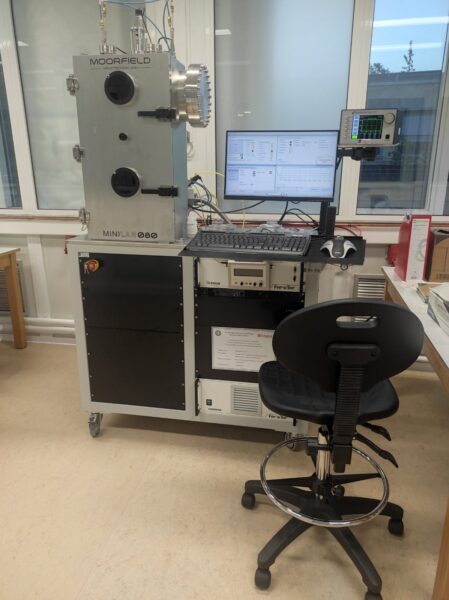
Minilab ET080A
e-Gun evaporation and thermal evaporation
Metals: Al, Au, Pt, Pd, Ag, Ti, Cr, Ru, Ni, Co.
6 pocket material target revolver for multilayer coatings without braking vacuum, from the e-Gun evaporation
Co-deposition of metals for alloys such as FeNi
e-Gun evaporation source: 5kW, up to 10 kV
Thermal evaporation source: 200A/8V
Substrates: Semiconductors, dielectrics, resists
From small samples of 1x1 cm2 to 8΄΄ wafers
Ohmic contacts, Metal electrodes and interconnects of semiconductor devices, etc.
SQC-310C (INFICON Instruments for Intelligent Control)
Manual mode: Measures the thickness of the film deposited on the wafer through quartz crystal microbalance (QCM)
Automatic mode: Perform evaporations through recipes


