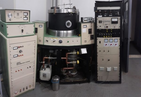
RF-S / Radio-Frequency Sputtering
Sputtering is a technique that belongs to the Physical Vapor Deposition procedures that are widely used in order to deposit thin films into various substrates. Sputtering effect takes place when ionizing gas molecules are employed in order to displace atoms from a specific material that is called target. The process of creating ions, electrons and neutral atoms in a mixture is called vaporization and is achieved by applying high voltage on the target material. In a magnetron sputtering configuration the voltage is delivered across a low-pressure gas in order to produce the high energy plasma. This plasma emits a light that is unique for each gas we use and it is called “glow discharge”.
The energetic plasma constituents strike the target that consists of the desired coating material. The force causes atoms to eject from the target material. Consequently, the sputtered atoms travel from the target to the substrate in order to create a thin film. Since sputtering takes place in a high-energy environment, it has the capability of producing strong bonds between the film and the substrate at atomic level. Sputtering is regarded as the most cost-effective technique with fair degree of accuracy, in terms of thickness and uniformity issues, for producing thin coatings.


Mantis Deposition Ltd
Radio-frequency (RF) magnetron sputtering
Metal oxides and metals
Base Pressure: 3 × 10⁻⁷ Torr
Process Pressure: 1 - 40 mTorr
Power: 20 – 300 Watt
Temperature: 20 – 550 oC
Ar and O2 flow rates: 1 – 100 sccm
From samples of 1x1 cm2 up to 3” wafer
Thin film deposition of various oxides (such as TiO2, Ta2O5, HfO2, SiO2, V2O5) as well metals (TiN, Ti, Mo, Ag, Cu, Pt) for Micro/Nanoelectronic devices including non-volatile memories, sensors and MEMS.
Dr. Panagiotis Bousoulas, panbous@mail.ntua.gr
Dr. Menelaos-Charalampos Tsigkourakos, mxtsig@gmail.com
Nordiko Ltd RFG2500
Radio-frequency (RF) diode & magnetron sputtering
Metals, nitrides, oxides
Base Pressure: <1x10⁻⁷ Torr
Process pressure: 2 - 30 mTorr
Power: 50 - 2500 Watt
Temperature: 20 – 350 οC
Ar, O2 and N2 flow rates: 1 – 100 sccm
From samples of 1 × 1 cm2 up to 2” wafer
Oxides & Nitrides for Transparent optoelectronics (ZnO, ITO, NiO, SiO2, GaN, AlN, ZnN, TaN) and oxide chromogenics for smart windows (VO2, WO3, NiO)
Elias Aperathitis, eaper@physics.uoc.gr
Emmanuel Gagaoudakis, mgagas@iesl.forth.gr


