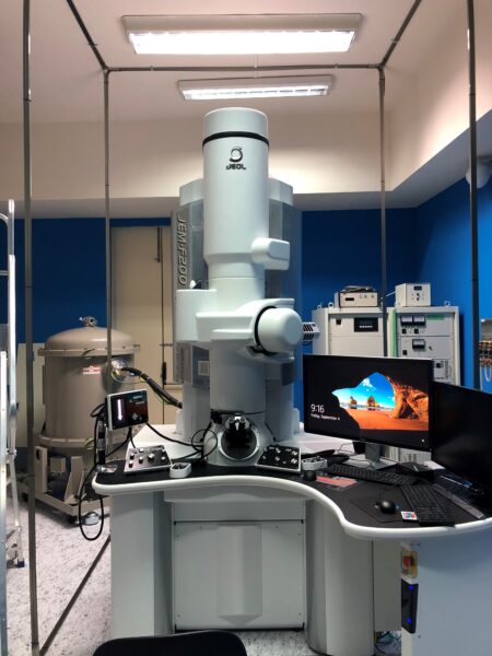
TEM /Transmission Electron Microscopy
EM and Scanning TEM (STEM) utilizes a high-energy electron beam that is transmitted through a very thin sample. In TEM, the beam is stationary while in STEM, a fine focused electron beam is scanned across the sample. The transmitted electrons are used to form images of the sample allowing morphology’s studies at the nanoscale. For crystalline samples, diffraction phenomena are exploited to obtain information about the sample’s crystallography. High-Resolution TEM & STEM (HRTEM & HRSTEM) provide images with atomic resolution (0.1-0.2 nm). These techniques are used to provide information about the arrangement of atoms on interfaces, surfaces and crystalline defects. Elemental analysis can be performed by Energy Dispersive X-ray (EDX) spectroscopy through analysis of the X-rays emitted by the sample. In addition, using Electron Energy Loss Spectroscopy & Energy Filtered TEM (EELS & EFTEM) chemical analysis and mapping can be extended to light atoms (down to Li) while chemical bonding and valency of atoms can be studied.
The facility includes 6 microscopes ranging from conventional TEM to HRTEM (0.19nm resolution) and HRSTEM (0.14nm resolution) including analytical TEM incorporating EDS and EELS/EFTEM.


Thermo Fisher Scientific Talos F200i TEM
Conventional & High Resolution Scanning / Transmission Electron Microscopy, Energy Dispersive X-ray Spectroscopy (EDX)
Field Emission Gun
200kV
16 Mpixel CETA CMOS camera
4kx4k STEM imaging
Triple Thermo-Fisher 3 detectors system bright field (BF), annular dark field (DF1,DF2)
Fischione 3000 high angle annular dark field detector (HAADF)
EDX Bruker 6|T Flash 100 mm2 (light elements sensitivity down to Be)
TEM point resolution: 0.25nm
TEM information limit: 0.12nm
STEM resolution: 0.16nm
x,y movement: α tilt = ± 35o, β tilt = ± 30o
4 available S/TEM detectors: HAADF, DF4, DF2, BF
max solid angle for EDX: 1.3srad
Dr. Nikos Boukos, n.boukos@inn.demokritos.gr
FEI CM20 TEM
Conventional & High Resolution Transmission Electron Microscopy, Electron Energy Loss Spectroscopy (EELS) and Energy Dispersive X-ray Spectroscopy (EDX) analysis
Thermionic gun LaB6
200kV
1M pixel CCD camera with GIF
EDAX EDX system (light elements sensitivity down to B)
GATAN GIF200 imaging filter
TEM point resolution: 0.27nm
TEM information limit: 0.18nm
x,y movement: α tilt = ± 45o, β tilt = ± 30o
Energy Filtered TEM
Dr. Nikos Boukos, n.boukos@inn.demokritos.gr
Jeol JEM-F200 Multi-purpose UHR TEM/STEM
High-Resolution Scanning/Transmission Electron Microscopy (HRTEM/HRSTEM), Energy Dispersive X-ray (EDX) Spectroscopy
Cold Field Emission Gun
200 kV
9Mp CMOS GATAN Bottom camera
4Mp JEOL side camera
In Stem mode: High Angle Annular Dark Field ( HAADF Z-contrast imaging), Annular Bright Field (ABF) and Annular Dark Field (ADF) imaging
EDX detector T-max 65 Oxford Instruments for Nanoanaysis & Chemical mapping
HRTEM point-to-point 0.19 nm
HRSTEM point-to-point 0.14 nm
x,y movement: α tilt = ± 25o, β tilt = ± 25o, high tilt retainer ± 65o
Professor Thomas Kehagias (kehagias@auth.gr)
Professor Philomela Komninou, Director (komnhnoy@auth.gr )
Jeol JEM 2011 UHR TEM
Conventional & High-Resolution Transmission Electron Microscopy, Energy Dispersive X-ray (EDX) Spectroscopy
Thermionic gun LaB6
200 kV
20 Mpixel CMOS camera XAROSA EmSis - Olympus
EDX detector T-max 65 Oxford Instruments
0.19 nm
x,y movement: α tilt = ± 12o, β tilt = ± 12o
Professor Thomas Kehagias, kehagias@auth.gr
Professor Philomela Komninou, komnhnoy@auth.gr
Jeol JEM 2000FX HR TEM
Conventional & High-Resolution Transmission Electron Microscopy
Thermionic gun LaB6
200 kV
1.4 Mpixel CCD camera KeenView G2 - Olympus
0.28 nm
x,y movement: α tilt = ± 30o, β tilt = ± 30o
Professor Thomas Kehagias, kehagias@auth.gr
Professor Philomela Komninou, komnhnoy@auth.gr
Jeol JEM 1010 TEM
Conventional Transmission Electron Microscopy
Thermionic gun W
100 kV
GATAN Compact TV camera – Model 696
0.40 nm
x,y movement: α tilt = ± 45o, β tilt = ± 45o
Professor Thomas Kehagias, kehagias@auth.gr
Professor Philomela Komninou, komnhnoy@auth.gr


